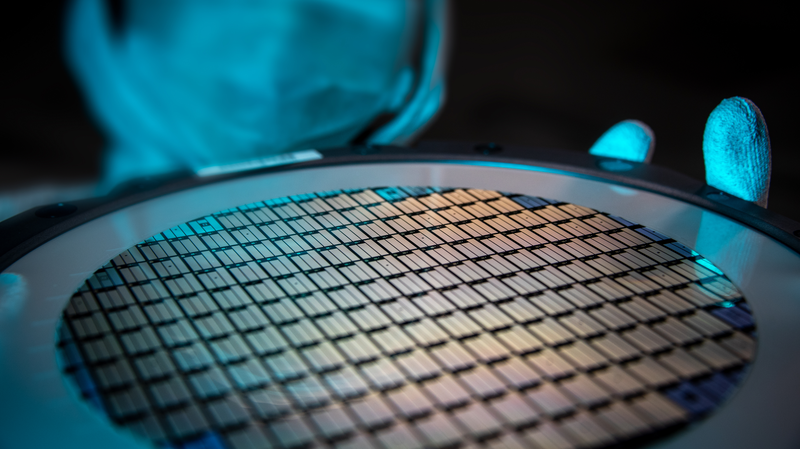
At the frontier of chip innovation, scientists from the Chinese mainland have developed a novel production technique for indium selenide—known as the “golden semiconductor”—that could redefine next-generation electronics. Published in Science, the study by Peking University and Renmin University of China outlines how a refined heating process accelerates crystal growth from the lab bench to wafer-scale manufacturing.
The crux of the challenge has been maintaining the perfect 1:1 atomic ratio of indium and selenium—any imbalance leads to defects that degrade performance. Professor Liu Kaihui of Peking University’s School of Physics explains: “By sealing amorphous indium selenide film with solid indium and applying controlled heat, vaporized atoms create an indium-rich liquid interface. This dynamic interface slowly transforms into a uniform, crystalline structure without ratio drift.”
With this approach, the team successfully fabricated 5-centimeter-diameter wafers and assembled large-scale arrays of high-performance transistors. Researcher Qiu Chengguang of Peking University’s School of Electronics adds: “These wafers are ready for direct integration into chip devices, marking a key step toward scalable manufacturing.”
Why it matters: As silicon-based chips approach their physical limits, indium selenide offers higher performance at lower energy costs. Experts predict these new wafers will power advancements in AI, autonomous driving, and smart devices, opening doors to more efficient data centers and edge computing.
Reviewers in Science hailed the work as “a major advancement in crystal growth,” underscoring its potential to reshape the semiconductor landscape.
Reference(s):
China develops new method to mass-produce high-quality semiconductors
cgtn.com